Wiring diagram recommended wire sizes terminals wire size solid stranded wire. Wiring diagram 1 4 2 3 s oli d 2 x 8 awg 84 mms tat e r ela y output input load 12 v.
Designing A Diversion Water Heater Load For Aux 1 Using An
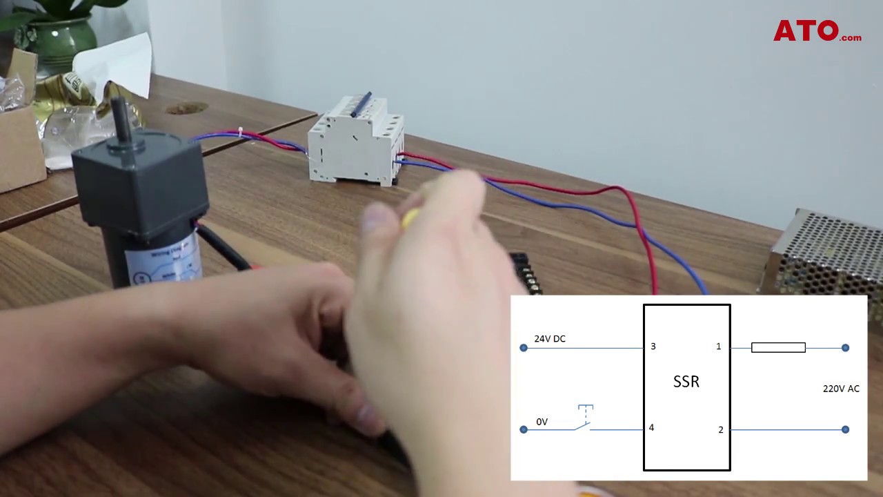
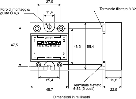
Crydom d1d40 wiring diagram. 100 vdc d1d07 d1d12 d1d20 d1d40 200 vdc d2d07 d2d12 d2d40 400 vdc d4d07 d4d12 500 vdc d5d07 d5d10 available options not all part number combinations are available. Equivalent circuit block diagrams ac ac ac trigger circuit current limiter ac 3 4 2 1 acdc converter 13 14 15 diagram. We have an input circuit rated 35 32 volts a dual type opto coupler and n channel power mosfet and various protection circuits. Equivalent circuit block diagrams ac ac ac trigger circuit current limiter ac 3 4 2 1 acdc converter 13 14 15 diagram. Input 2 x 12 awg 33 mm2 output 2 x 8 awg 84 mm 2. Series 1 ac control dc dc ac.
3 illustrates how the above ideas come together with the crydom d1d40 type ssrs. Choose wire gauge according to actual load current. Series 1 ac ac ac ac trigger circuit current limiter ac 3 2 1 acdc converter 12 humidity per iec60068 2 78 93 non condensing mtbf mean time between failures at 40c ambient temperature 10 11641553 hours 1328 years. Equivalent circuit block diagrams diagram. Contact crydom technical support for information on the availability of a specific part number. Wiring diagrams b wire size maximum wire size capacity per terminal.
Equivalent circuit block diagrams dc dc dc trigger circuit control circuit dc 4 3 1 2 0 2 4 6 8 10 12 14 0 5 10 15 20 25 30 35 input current vs input voltage. For larger wire sizes use lug terminals see table 1 for available part numbers. Series 1 dc dc dc ac trigger circuit current limiter ac 3 4 2 1 12 diagram. Series 1 ac control dc dc ac. Wiring diagram 1 4 2 3 s oli d s tat e r ela y output input load 12 v 4 3. Contact crydom technical support for information on.
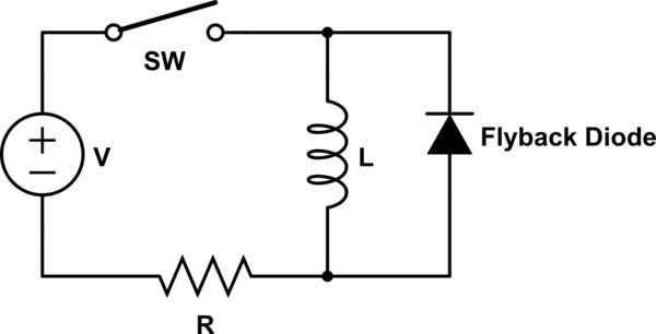
Contact crydom technical support for information on. Wiring diagram 1 4 2 3 s oli d s tat e r ela y output input load v v 1 4 s oli d s tat e r ela y output input v v load inductive loads must be diode suppresed.
Gallery of Crydom D1d40 Wiring Diagram